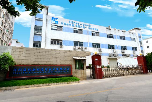
Hiner-pack was founded in 2013,it is a high-tech enterprise which is integrated Design,R&D,Manufacturing,Sales of IC packaging and testing as well as semiconductive wafer fabrication process in automated handling,carrying,transportation to provide customers turnkey services.
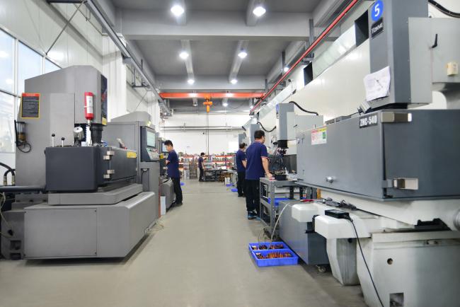
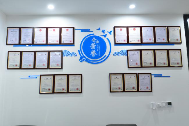
Hiner-pack has established a depth of cooperation with well-known enterprises and built a polymer material R&D base with domestic well-known universities as well as scientific research institutions.Hiner-pack has mastered special processing technique and manufacturing in semiconductor packaging raw material field.Owned a lot of inventions and practical new patents.Through years of unremitting efforts,Hiner-pack has a professional R&D team to improve semiconductor packaging products, new products continue to launch,and to solve the customer demand for high quality products.
Learn more through our official website https://www.hiner-pack.com/english/