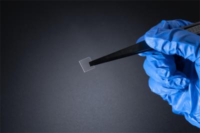
GaN Epitaxial Wafer
(69)
Fe Doped GaN Substrates Resistivity > 10⁶ Ω·Cm RF Devices
Price: Negotiable
MOQ: Negotiable
Delivery Time: 3-4 week days
Brand: GaNova
High Light:ISO GaN Substrates, gan semiconductor wafer, Fe Doped GaN Substrates
2inch C-face Fe-doped SI-type free-standing GaN single crystal substrate Resistivity > 106 Ω·cm RF devices The achieved breakdown voltage of the Fe-doped GaN epitaxial layer can be as high as 2457 V, which is attributed to the Fe-doped GaN epitaxial layer with higher resistance, which can sustain... View More
Contact Now
GaN Single Crystal Substrate
Price: Negotiable
MOQ: Negotiable
Delivery Time: 3-4 week days
Brand: GaNova
High Light:GaN Single Crystal Substrate, gan epi wafer 400um, UKAS Single Crystal Substrate
2inch C-face Si-doped n-type free-standing GaN single crystal substrate Resistivity < 0.05 Ω·cm Power device/laser wafer Overview One of the key methods used to fabricate these devices is a light n-type doping of GaN with a low residual impurity concentration of the order of 1015 cm−3 or less. De... View More
Contact Now
4 Inch P-Type Mg-Doped GaN On Sapphire Wafer SSP Resistivity~10Ω Cm LED Laser PIN Epitaxial Wafer
Price: Negotiable
MOQ: Negotiable
Delivery Time: 3-4 week days
Brand: GaNova
High Light:LED Laser PIN Epitaxial Wafer
4 inch P-type Mg-doped GaN on sapphire wafer SSP resistivity~10Ω cm LED, laser, PIN epitaxial wafer The electrical properties of p-type Mg-doped GaN are investigated through variable-temperature Hall effect measurements. Samples with a range of Mg-doping concentrations were prepared by metalorganic ... View More
Contact Now
625um To 675um 4 Inch Blue LED GaN Epitaxial Wafer On Sapphire SSP Flat Sapphire
Price: Negotiable
MOQ: Negotiable
Delivery Time: 3-4 week days
Brand: GaNova
High Light:625um GaN Epitaxial Wafer, SSP gan on sapphire wafers, 675um GaN Epitaxial Wafer
Substrate Thickness 650 ± 25 μm 4 Inch Blue LED GaN Epitaxial Wafer On Sapphire SSP Flat Sapphire 4 inch Blue LED GaN epitaxial wafer on sapphire SSP For example, GaN is the substrate which makes violet (405 nm) laser diodes possible, without use of nonlinear optical frequency-doubling. Its sensitiv... View More
Contact Now

2 Inch Green LED GaN On Silicon Wafer Dimension 520±10nm
Price: Negotiable
MOQ: Negotiable
Delivery Time: 3-4 week days
Brand: GaNova
High Light:2 Inch GaN On Silicon Wafer, Green LED GaN On Silicon Wafer, 520nm GaN On Silicon Wafer
2inch Green-LED GaN on silicon wafer Overview Gallium nitride (GaN) is creating an innovative shift throughout the power electronics world. For decades, silicon-based MOSFETs (Metal Oxide Semiconductor Field Effect Transistors) have been an integral part of the everyday modern world that helps conve... View More
Contact Now
10 X 10.5 Mm2 C Face Un Doped N Type Free Standing GaN Single Crystal Substrate
Price: Negotiable
MOQ: Negotiable
Delivery Time: 3-4 week days
Brand: GaNova
High Light:Un-Doped GaN Single Crystal Substrate, Free-Standing GaN Single Crystal Substrate, N Type GaN Single Crystal Substrate
10*10.5mm² C-face Un-doped n-type free-standing GaN single crystal substrate Resistivity < 0.1 Ω·cm Power device/laser Overview Premium quality GaN crystal substrates with low dislocation density (on the order of 105 /cm2) and uniform surface with no periodic defects. These high quality GaN cryst... View More
Contact Now
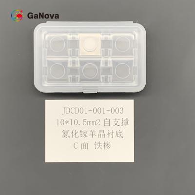
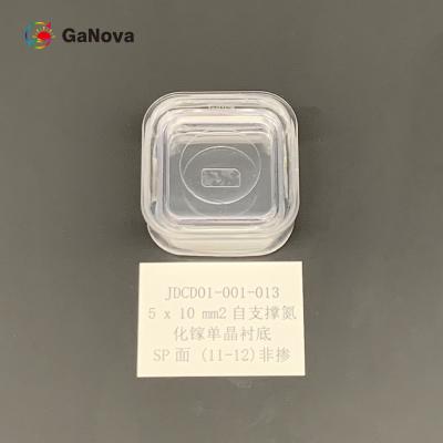
10*10.5mm2 C-Face Fe-Doped SI-Type Free-Standing GaN Single Crystal Substrate Macro Defect Density 0cm⁻² TTV ≤ 10 Μm Resistivity 10⁶ Ω·Cm RF Devices Wafer
Price: Negotiable
MOQ: Negotiable
Delivery Time: 3-4 week days
Brand: GaNova
High Light:GaN Single Crystal Substrate, 10*10.5mm2 GaN Single Crystal Substrate
10*10.5mm2 C-face Fe-doped SI-type free-standing GaN single crystal substrate Resistivity > 106 Ω·cm RF devices wafer Overview We sell directly from the factory, and therefore can offer the best prices on the market for high quality GaN crystal substrates. Customers from all over the world have t... View More
Contact Now
10 X 10.5 Mm2 Free Standing GaN Substrates - 10 Μm ≤ BOW ≤ 10 Μm
Price: Negotiable
MOQ: Negotiable
Delivery Time: 3-4 week days
Brand: GaNova
High Light:Free Standing GaN Substrates, 10 X 10.5 mm2 GaN Substrates
10*10.5mm² C-face Un-doped n-type free-standing GaN single crystal substrate Resistivity < 0.1 Ω·cm Power device/laser Applications Laser diodes: violet LD, blue LD, and green LD Power electronic devices, High frequency electronic devices More than 10 years of wafer fabrication technology experie... View More
Contact Now
TTV ≤ 10µm A-Face Un-Doped N-Type Free-Standing GaN Single Crystal Substrate Resistivity 0.1 Ω·cm Power Device/Laser W
Price: Negotiable
MOQ: Negotiable
Delivery Time: 3-4 week days
Brand: GaNova
High Light:Laser W GaN Single Crystal Substrate, Power Device GaN Single Crystal Substrate, Free Standing GaN Single Crystal Substrate
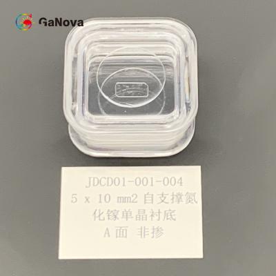
5*10mm2 A-face Un-doped n-type free-standing GaN single crystal substrate Resistivity < 0.1 Ω·cm Power device/laser wafer Overview Gallium nitride (GaN) is a very hard, mechanically stable wide bandgap semiconductor. With higher breakdown strength, faster switching speed, higher thermal conductiv... View More
Contact Now

350 ±25µm Thickness Un-Doped N-Type Free-Standing GaN Single Crystal Substrate with TTV ≤ 10µm and Resistivity 0.1 Ω·cm
Price: Negotiable
MOQ: Negotiable
Delivery Time: 3-4 week days
Brand: GaNova
High Light:10µm GaN Single Crystal Substrate, GaN Single Crystal Substrate
5*10mm2 SP-face (20-21)/(20-2-1) Un-doped n-type free-standing GaN single crystal substrate Resistivity < 0.1 Ω·cm Power device/laser wafer Overview Gallium Nitride (GaN) substrate is a high-quality single-crystal substrate. It is made with original HVPE method and wafer processing technology, wh... View More
Contact Now
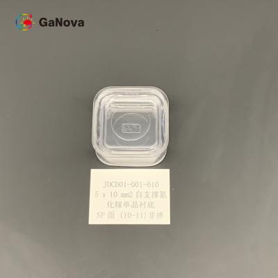
5*10mm2 SP-Face 10-11 Un-Doped N-Type Free-Standing GaN Single Crystal Substrate 0.1 Ω·cm Resistivity For Power Device
Price: Negotiable
MOQ: Negotiable
Delivery Time: 3-4 week days
Brand: GaNova
High Light:0.1 Ω·cm GaN Single Crystal Substrate, 5*10mm2 GaN Single Crystal Substrate
5*10.5mm2 SP-face (10-11) Un-doped n-type free-standing GaN single crystal substrate Resistivity < 0.1 Ω·cm Power device/laser wafer Generative adversarial networks (GANs) are algorithmic architectures that use two neural networks, pitting one against the other (thus the “adversarial”) in order t... View More
Contact Now
5x10mm2 SP-Face 10-11 Un-Doped N-Type Free-Standing GaN Single Crystal Substrate with TTV ≤ 10µm Resistivity 0.05 Ω·cm
Price: Negotiable
MOQ: Negotiable
Delivery Time: 3-4 week days
Brand: GaNova
High Light:Free-Standing GaN Single Crystal Substrate, 5x10mm2 GaN Single Crystal Substrate
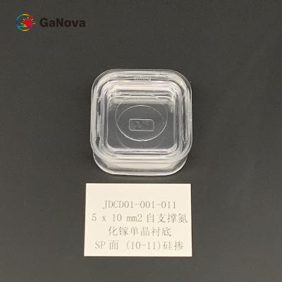
5*10mm2 SP-face (10-11) Un-doped n-type free-standing GaN single crystal substrate Resistivity < 0.05 Ω·cm Power device/laser wafer Overview GaN has many serious advantages over silicon, being more power efficient, faster, and even better recovery characteristics. However, while GaN may seem like... View More
Contact Now
Macro Defect Density 0cm⁻² Un-Doped SI-Type Free-Standing GaN Single Crystal Substrate For RF Devices 5*10mm2 M-Face
Price: Negotiable
MOQ: Negotiable
Delivery Time: 3-4 week days
Brand: GaNova
High Light:RF Devices GaN Single Crystal Substrate, 5*10mm2 GaN Single Crystal Substrate, Free Standing GaN Single Crystal Substrate
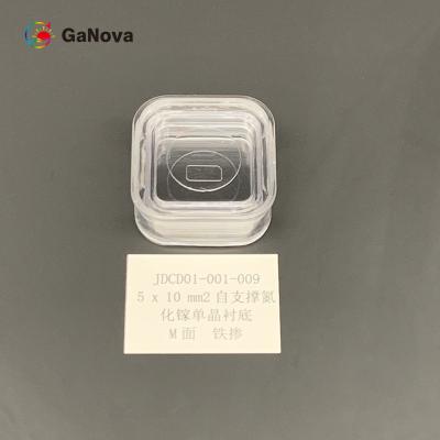
5*10mm2 M-face Un-doped SI-type free-standing GaN single crystal substrate Resistivity > 106 Ω·cm RF devices wafer Overview Thin Epi wafers are commonly used for leading edge MOS devices. Thick Epi or Multi-layered epitaxial wafers are used for the devices mainly to control electric power, and th... View More
Contact Now
SP-Face 11-12 Un-Doped N-Type Free-Standing GaN Single Crystal Substrate Resistivity 0.05 Ω·cm Macro Defect Density 0cm⁻²
Price: Negotiable
MOQ: Negotiable
Delivery Time: 3-4 week days
Brand: GaNova
High Light:0.05 Ω·cm GaN Single Crystal Substrate, Un-Doped GaN Single Crystal Substrate
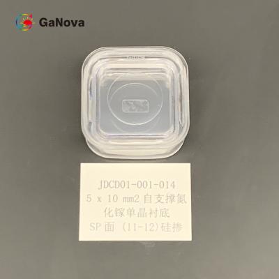
5*10mm2 SP-face (11-12) Un-doped n-type free-standing GaN single crystal substrate Resistivity < 0.05 Ω·cm Power device/laser wafer Overview Because GaN transistors are able to turn on faster than silicon transistors, they are able to reduce the losses caused by this transition. Another way that ... View More
Contact Now
Power Device 5x10mm2 Un-Doped N-Type Free-Standing GaN Single Crystal Substrate with Resistivity 0.1 Ω·cm and BOW within 10µm
Price: Negotiable
MOQ: Negotiable
Delivery Time: 3-4 week days
Brand: GaNova
High Light:0.1 Ω·cm GaN Single Crystal Substrate, 10µm GaN Single Crystal Substrate, 5x10mm2 GaN Single Crystal Substrate
5*10mm2 SP-face (11-12) Un-doped n-type free-standing GaN single crystal substrate Resistivity < 0.1 Ω·cm Power device Overview Since the 1990s, it has been used commonly in light emitting diodes (LED). Gallium nitride gives off a blue light used for disc-reading in Blu-ray. Additionally, gallium... View More
Contact Now
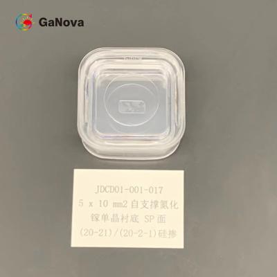
5*10mm2 SP-Face Un-Doped N-Type Free-Standing GaN Single Crystal Substrate 20-21 / 20-2-1 10mm2 Resistivity 0.05 Ω·cm
Price: Negotiable
MOQ: Negotiable
Delivery Time: 3-4 week days
Brand: GaNova
High Light:0.05 Ω·cm GaN Single Crystal Substrate, 10mm2 GaN Single Crystal Substrate, 20-21 GaN Single Crystal Substrate
5*10mm2 SP-face (20-21)/(20-2-1) Un-doped n-type free-standing GaN single crystal substrate Resistivity < 0.05 Ω·cm Power device/laser wafer Overview A generative adversarial network (GAN) has two parts: The generator learns to generate plausible data. The generated instances become negative trai... View More
Contact Now
Dimension 520±10nm 2inch Green-LED GaN On Silicon Wafer 20nmContact Layer
Price: Negotiable
MOQ: Negotiable
Delivery Time: 3-4 week days
Brand: GaNova
High Light:20nm GaN On Silicon Wafer, 520±10nm GaN On Silicon Wafer
2inch Green-LED GaN on silicon wafer Overview Gallium nitride (GaN) is creating an innovative shift throughout the power electronics world. For decades, silicon-based MOSFETs (Metal Oxide Semiconductor Field Effect Transistors) have been an integral part of the everyday modern world that helps conve... View More
Contact Now
2inch Blue-LED GaN On Silicon Wafer Longueur D’Onde Laser 455±10nm
Price: Negotiable
MOQ: Negotiable
Delivery Time: 3-4 week days
Brand: GaNova
High Light:455±10nm GaN On Silicon Wafer
2inch Blue-LED GaN on silicon wafer Gallium Nitride is a semiconductor technology used for high power, high-frequency semiconductor applications. Gallium Nitride exhibits several characteristics that make it better than GaAs and Silicon for various high power components. These characteristics includ... View More
Contact Now
2inch C-Face Fe-Doped SI-Type Free-Standing GaN Single Crystal Substrate Resistivity > 10⁶ Ω·cm RF Devices
Price: Negotiable
MOQ: Negotiable
Delivery Time: 3-4 week days
Brand: Nanowin
High Light:2inch GaN Single Crystal Substrate, Resistivity GaN Single Crystal Substrate
2inch C-face Fe-doped SI-type free-standing GaN single crystal substrate Resistivity > 106 Ω·cm RF devices Overview Gallium Nitride (GaN) epitaxial wafers (epi-wafers). GaN high-electron-mobility transistors (HEMT) wafers on different substrates such as silicon substrate, sapphire substrate, sili... View More
Contact Now

4-Inch Mg-Doped GaN/Sapphire Substrates SSP Resistivity~10Ω cm LED Laser PIN Epitaxial Wafer
Price: Negotiable
MOQ: Negotiable
Delivery Time: 3-4 week days
Brand: GaNova
High Light:LED Laser GaN Epitaxial Wafer
4 inch P-type Mg-doped GaN on sapphire wafer SSP resistivity~10Ω cm LED, laser, PIN epitaxial wafer Why Use GaN Wafers? Gallium Nitride on sapphire is the ideal material for radio energy amplification. It offers a number of benefits over silicon, including a higher breakdown voltage and better perfo... View More
Contact Now