
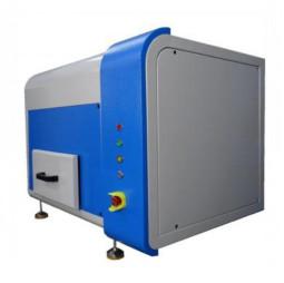
Boost Production Rapid Thermal Processing RTP-SA-8 Annealing System
Price: Negotiable
MOQ: Negotiable
Delivery Time: 3 month
Brand: Ganova
High Light:Boost Production Rapid Thermal Processing, Rapid Thermal Processing Annealing System
1.Basic configuration of equipment system 1.1outline The Rapid Thermal Processing is a vertical semi-automatic 8-inch wafer rapid annealing furnace, which uses two layers of infrared halogen lamps as heat sources for heating. The internal quartz cavity is insulated and insulated, and the outer shell... View More
➤ Visit Website
150mm Rapid Thermal Annealing System With Three Sets Process Gases
Price: Negotiable
MOQ: 1
Delivery Time: 8-10week days
Brand: GaNova
High Light:150mm Rapid Thermal Annealing System, desktop rapid thermal processing equipment, Wafer Rapid Thermal Annealing System
RTP-150RL Rapid Thermal Annealing System with Three Sets Process Gases RTP-150RL: Is in the protection atmosphere of the desktop manual rapid annealing system, with infrared visible light heating single piece Wafer or sample, short process time, high temperature control precision, suitable for 2-6 i... View More
➤ Visit Website

JDCD05-001-003 10*10mm2*0.3mm Electronic Grade Single Crystal Diamond,N Content<100ppb, XRD<0.015º Thermal Conductivity
Price: Negotiable
MOQ: Negotiable
Delivery Time: 3-4 week days
Brand: GaNova
High Light:Electronic Grade Single Crystal Diamond, 10*10mm2*0.3mm Single Crystal Diamond
10*10mm2*0.3mm electronic grade single crystal diamond,N content View More
➤ Visit Website

JDCD05-001-006 10*10mm2*0.5mm Electronic Grade Single Crystal Diamond,N Content<100ppb, XRD<0.015º Thermal Conductivity
Price: Negotiable
MOQ: Negotiable
Delivery Time: 3-4 week days
Brand: GaNova
High Light:10*10mm2*0.5mm Single Crystal Diamond
JDCD05-001-006 10*10mm2*0.5mm electronic grade single crystal diamond,N content View More
➤ Visit Website
Fe Doped GaN Substrates Resistivity > 10⁶ Ω·Cm RF Devices
Price: Negotiable
MOQ: Negotiable
Delivery Time: 3-4 week days
Brand: GaNova
High Light:ISO GaN Substrates, gan semiconductor wafer, Fe Doped GaN Substrates
2inch C-face Fe-doped SI-type free-standing GaN single crystal substrate Resistivity > 106 Ω·cm RF devices The achieved breakdown voltage of the Fe-doped GaN epitaxial layer can be as high as 2457 V, which is attributed to the Fe-doped GaN epitaxial layer with higher resistance, which can sustain... View More
➤ Visit Website
GaN Single Crystal Substrate
Price: Negotiable
MOQ: Negotiable
Delivery Time: 3-4 week days
Brand: GaNova
High Light:GaN Single Crystal Substrate, gan epi wafer 400um, UKAS Single Crystal Substrate
2inch C-face Si-doped n-type free-standing GaN single crystal substrate Resistivity < 0.05 Ω·cm Power device/laser wafer Overview One of the key methods used to fabricate these devices is a light n-type doping of GaN with a low residual impurity concentration of the order of 1015 cm−3 or less. De... View More
➤ Visit Website
4 Inch P-Type Mg-Doped GaN On Sapphire Wafer SSP Resistivity~10Ω Cm LED Laser PIN Epitaxial Wafer
Price: Negotiable
MOQ: Negotiable
Delivery Time: 3-4 week days
Brand: GaNova
High Light:LED Laser PIN Epitaxial Wafer
4 inch P-type Mg-doped GaN on sapphire wafer SSP resistivity~10Ω cm LED, laser, PIN epitaxial wafer The electrical properties of p-type Mg-doped GaN are investigated through variable-temperature Hall effect measurements. Samples with a range of Mg-doping concentrations were prepared by metalorganic ... View More
➤ Visit Website

JDCD05-001-005 5*5mm2*0.5mm Electronic Grade Single Crystal Diamond,N Content<100ppb, XRD<0.015º Thermal Conductivity
Price: Negotiable
MOQ: Negotiable
Delivery Time: 3-4 week days
Brand: GaNova
High Light:XRD<0.015º Single Crystal Diamond
JDCD05-001-005 5*5mm2*0.5mm electronic grade single crystal diamond,N content View More
➤ Visit Website
625um To 675um 4 Inch Blue LED GaN Epitaxial Wafer On Sapphire SSP Flat Sapphire
Price: Negotiable
MOQ: Negotiable
Delivery Time: 3-4 week days
Brand: GaNova
High Light:625um GaN Epitaxial Wafer, SSP gan on sapphire wafers, 675um GaN Epitaxial Wafer
Substrate Thickness 650 ± 25 μm 4 Inch Blue LED GaN Epitaxial Wafer On Sapphire SSP Flat Sapphire 4 inch Blue LED GaN epitaxial wafer on sapphire SSP For example, GaN is the substrate which makes violet (405 nm) laser diodes possible, without use of nonlinear optical frequency-doubling. Its sensitiv... View More
➤ Visit Website

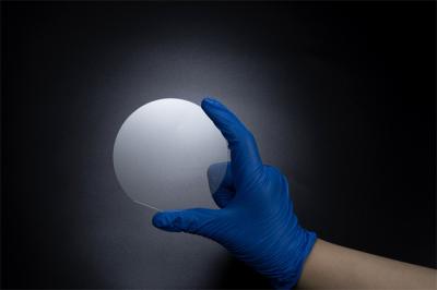
JDCD08-001-006 6inch C-Plane Sapphire Substrate Wafer
Price: Negotiable
MOQ: Negotiable
Delivery Time: Negotiable
High Light:6inch Sapphire Substrate Wafer
JDCD08-001-006 6inch C-Plane Sapphire Substrate Wafer Sapphires are Second Only to Diamonds in Durability Diamond is the most durable naturally occurring element on earth and ranks as a 10 out of 10 on Mohs Scale of Mineral Hardness. Sapphires are also very durable and rank as a 9 out of 10 on Mohs ... View More
➤ Visit Website

JDCD05-001-007 CVD Diamond Substrates
Price: Negotiable
MOQ: Negotiable
Delivery Time: 3-4 week days
Brand: GaNova
High Light:CVD Diamond Substrates, CVD Diamond Substrates 007
JDCD05-001-007 CVD Diamond Substrates Overview Diamond is a unique material that often exhibits extreme properties compared to other materials. Discovered about 30 years ago, the use of hydrogen in plasma-enhanced chemical vapor deposition (CVD) has enabled the growth and coating of diamond in film ... View More
➤ Visit Website

4inch 4H-SiC substrate P-level SI 500.0±25.0μm MPD≤5/cm2 Resistivity≥1E5Ω·cm for power and microwave
Price: Negotiable
MOQ: Negotiable
Delivery Time: 3-4 week days
Brand: GaNova
JDCD03-002-002 4inch 4H-SiC substrate P-level SI 500.0±25.0μm MPD≤5/cm2 Resistivity≥1E5Ω·cm for power and microwave devices Overview SiC is used for the fabrication of very high-voltage and high-power devices such as diodes, power transistors, and high power microwave devices. Compared to convention... View More
➤ Visit Website

8 inch Wafer Dicing Machine X Axis Cutting Range 260mm 1.8 KW 2.2 KW
Price: Negotiable
MOQ: 1
Delivery Time: 8-10week days
Brand: GaNova
High Light:8 inch Wafer Dicing Machine, wafer cutting machine 260mm, Wafer Dicing Machine X Axis
DAD3350 Wafer Dicing Machine X-Axis Cutting Range 260mm 1.8 KW, 2.2 KW Process quality By adopting a high-rigidity bridge-type frame and a spindle front-section support structure, which prevents heat shrinkage and vibration, a more stable processing point can be achieved. Process controls Auto align... View More
➤ Visit Website

Patterned Sapphire Crystal Wafer 2inch Sapphire Substrate
Price: Negotiable
MOQ: 1
Delivery Time: Negotiable
Brand: GaNova
High Light:Patterned sapphire crystal wafer, 2inch Sapphire Substrate, Al203 sapphire crystal wafer
A-Plane±0.2o Patterned Sapphire Substrates BOW≤-8~0μM Back Surface Roughness 0.8~1.2μm 2inch Patterned Sapphire Substrates,LED Chip,Substrate Material The regular patterns created on the sapphire substrate counteracts the effect of the total internal reflection at the GaN/sapphire interface. And, th... View More
➤ Visit Website

100.0mm Silicon Carbide Crystal 4" P Grade 18.0mm
Price: Negotiable
MOQ: Negotiable
Delivery Time: 3-4 week days
High Light:100.0mm Silicon Carbide Crystal, single crystal sic 4", Silicon Carbide Crystal 18.0mm
100.0mm±0.5mm SiC Seed Crystal 4" P Grade 0.015~0.028ohm.cm 18.0mm±2.0mm SiC Seed Crystal 4" PGrade Electronic devices formed in SiC can operate at extremely high temperatures without suffering from intrinsic conduction effects becauseof the wide energy bandgap. Also, this property allows ... View More
➤ Visit Website

2inch GaAs Epi Wafer GaAs Undoped Substrates VGF
Price: Negotiable
MOQ: Negotiable
Delivery Time: 3-4 week days
Brand: GaNova
High Light:GaAs Epi Wafer Undoped Substrates, GaAs-Si Wafer 2inch, 2inch GaAs Epi Wafer
GaAs-Si Wafer 2inch GaAs (100) Undoped Substrates EJ[0-1-1]±0.5° Overview GaAs applications cover a large variety of transistors for industry spanning optical fiber communication, wireless networks (WLAN), mobile handsets, blue tooth communications, satellite communications, monolithic microwave int... View More
➤ Visit Website
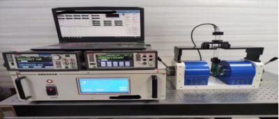
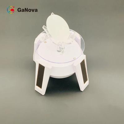
Semiconductor Materials Hall Effect Sensor Tester Carrier Concentration Measurement
Price: Negotiable
MOQ: 1
Delivery Time: 8-10week days
Brand: GaNova
High Light:Semiconductor Hall Effect Sensor Tester, electronic measurement equipment, Hall Effect Sensor Tester OEM
Semiconductor Materials Hall Effect Tester Carrier Concentration Measurement Product Overview: Hall effect tester is used to measure the carrier concentration, mobility, resistivity, Hall coefficient and other important parameters, and these parameters of semiconductor materials to understand the el... View More
➤ Visit Website
Dimension 520±10nm 2inch Green-LED GaN On Silicon Wafer 20nmContact Layer
Price: Negotiable
MOQ: Negotiable
Delivery Time: 3-4 week days
Brand: GaNova
High Light:20nm GaN On Silicon Wafer, 520±10nm GaN On Silicon Wafer
2inch Green-LED GaN on silicon wafer Overview Gallium nitride (GaN) is creating an innovative shift throughout the power electronics world. For decades, silicon-based MOSFETs (Metal Oxide Semiconductor Field Effect Transistors) have been an integral part of the everyday modern world that helps conve... View More
➤ Visit Website
2inch Blue-LED GaN On Silicon Wafer Longueur D’Onde Laser 455±10nm
Price: Negotiable
MOQ: Negotiable
Delivery Time: 3-4 week days
Brand: GaNova
High Light:455±10nm GaN On Silicon Wafer
2inch Blue-LED GaN on silicon wafer Gallium Nitride is a semiconductor technology used for high power, high-frequency semiconductor applications. Gallium Nitride exhibits several characteristics that make it better than GaAs and Silicon for various high power components. These characteristics includ... View More
➤ Visit Website

JDCD06-001-002 3-Inch Silicon Wafer MEMS Devices, Integrated Circuits,Dedicated Substrates For Discrete Devices
Price: Negotiable
MOQ: 1
Delivery Time: 3-4 week days
Brand: GaNova
High Light:Integrated Circuits Silicon Wafer, Discrete Devices Silicon Wafer
3-inch silicon wafer MEMS devices, integrated circuits,dedicated substrates for discrete devices Overview Silicon wafers act as a substrate for microelectronic devices and are especially useful in building electronic circuits because of their conductivity and affordability. Silicon comes seventh as ... View More
➤ Visit Website