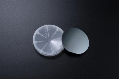
GaN Epitaxial Wafer
(68)
Fe Doped GaN Substrates Resistivity > 10⁶ Ω·Cm RF Devices
Price: Negotiable
MOQ: Negotiable
Delivery Time: 3-4 week days
Brand: GaNova
High Light:ISO GaN Substrates, gan semiconductor wafer, Fe Doped GaN Substrates
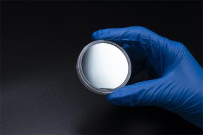
2inch C-face Fe-doped SI-type free-standing GaN single crystal substrate Resistivity > 106 Ω·cm RF devices The achieved breakdown voltage of the Fe-doped GaN epitaxial layer can be as high as 2457 V, which is attributed to the Fe-doped GaN epitaxial layer with higher resistance, which can sustain... View More
➤ Visit Website
GaN Single Crystal Substrate
Price: Negotiable
MOQ: Negotiable
Delivery Time: 3-4 week days
Brand: GaNova
High Light:GaN Single Crystal Substrate, gan epi wafer 400um, UKAS Single Crystal Substrate
2inch C-face Si-doped n-type free-standing GaN single crystal substrate Resistivity < 0.05 Ω·cm Power device/laser wafer Overview One of the key methods used to fabricate these devices is a light n-type doping of GaN with a low residual impurity concentration of the order of 1015 cm−3 or less. De... View More
➤ Visit Website
4 Inch P-Type Mg-Doped GaN On Sapphire Wafer SSP Resistivity~10Ω Cm LED Laser PIN Epitaxial Wafer
Price: Negotiable
MOQ: Negotiable
Delivery Time: 3-4 week days
Brand: GaNova
High Light:LED Laser PIN Epitaxial Wafer
4 inch P-type Mg-doped GaN on sapphire wafer SSP resistivity~10Ω cm LED, laser, PIN epitaxial wafer The electrical properties of p-type Mg-doped GaN are investigated through variable-temperature Hall effect measurements. Samples with a range of Mg-doping concentrations were prepared by metalorganic ... View More
➤ Visit Website
625um To 675um 4 Inch Blue LED GaN Epitaxial Wafer On Sapphire SSP Flat Sapphire
Price: Negotiable
MOQ: Negotiable
Delivery Time: 3-4 week days
Brand: GaNova
High Light:625um GaN Epitaxial Wafer, SSP gan on sapphire wafers, 675um GaN Epitaxial Wafer
Substrate Thickness 650 ± 25 μm 4 Inch Blue LED GaN Epitaxial Wafer On Sapphire SSP Flat Sapphire 4 inch Blue LED GaN epitaxial wafer on sapphire SSP For example, GaN is the substrate which makes violet (405 nm) laser diodes possible, without use of nonlinear optical frequency-doubling. Its sensitiv... View More
➤ Visit Website
Dimension 520±10nm 2inch Green-LED GaN On Silicon Wafer 20nmContact Layer
Price: Negotiable
MOQ: Negotiable
Delivery Time: 3-4 week days
Brand: GaNova
High Light:20nm GaN On Silicon Wafer, 520±10nm GaN On Silicon Wafer
2inch Green-LED GaN on silicon wafer Overview Gallium nitride (GaN) is creating an innovative shift throughout the power electronics world. For decades, silicon-based MOSFETs (Metal Oxide Semiconductor Field Effect Transistors) have been an integral part of the everyday modern world that helps conve... View More
➤ Visit Website
2inch Blue-LED GaN On Silicon Wafer Longueur D’Onde Laser 455±10nm
Price: Negotiable
MOQ: Negotiable
Delivery Time: 3-4 week days
Brand: GaNova
High Light:455±10nm GaN On Silicon Wafer
2inch Blue-LED GaN on silicon wafer Gallium Nitride is a semiconductor technology used for high power, high-frequency semiconductor applications. Gallium Nitride exhibits several characteristics that make it better than GaAs and Silicon for various high power components. These characteristics includ... View More
➤ Visit Website
2inch C-Face Fe-Doped SI-Type Free-Standing GaN Single Crystal Substrate Resistivity > 10⁶ Ω·cm RF Devices
Price: Negotiable
MOQ: Negotiable
Delivery Time: 3-4 week days
Brand: Nanowin
High Light:2inch GaN Single Crystal Substrate, Resistivity GaN Single Crystal Substrate
2inch C-face Fe-doped SI-type free-standing GaN single crystal substrate Resistivity > 106 Ω·cm RF devices Overview Gallium Nitride (GaN) epitaxial wafers (epi-wafers). GaN high-electron-mobility transistors (HEMT) wafers on different substrates such as silicon substrate, sapphire substrate, sili... View More
➤ Visit Website

4-Inch Mg-Doped GaN/Sapphire Substrates SSP Resistivity~10Ω cm LED Laser PIN Epitaxial Wafer
Price: Negotiable
MOQ: Negotiable
Delivery Time: 3-4 week days
Brand: GaNova
High Light:LED Laser GaN Epitaxial Wafer
4 inch P-type Mg-doped GaN on sapphire wafer SSP resistivity~10Ω cm LED, laser, PIN epitaxial wafer Why Use GaN Wafers? Gallium Nitride on sapphire is the ideal material for radio energy amplification. It offers a number of benefits over silicon, including a higher breakdown voltage and better perfo... View More
➤ Visit Website
4 Inch N-Type UID-Doped GaN On Sapphire Wafer SSP Resistivity>0.5 Ω cm LED, Laser, PIN Epitaxial Wafer
Price: Negotiable
MOQ: Negotiable
Delivery Time: 3-4 week days
Brand: GaNova
High Light:PIN GaN On Sapphire Wafer, 4 Inch GaN On Sapphire Wafer
4 inch N-type UID-doped GaN on sapphire wafer SSP resistivity>0.5 Ω cm LED, laser, PIN epitaxial wafer For example, GaN is the substrate which makes violet (405 nm) laser diodes possible, without use of nonlinear optical frequency-doubling. Its sensitivity to ionizing radiation is low (like other gr... View More
➤ Visit Website
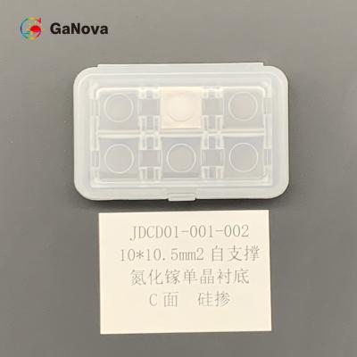
10*10.5mm2 GaN Single Crystal Substrate Thickness 350 ±25 µm TTV ≤ 10 µm
Price: Negotiable
MOQ: Negotiable
Delivery Time: 3-4 week days
Brand: GaNova
High Light:10*10.5mm2 GaN Single Crystal Substrate
10*10.5mm2 C-face Si-doped n-type free-standing GaN single crystal substrate Resistivity < 0.05 Ω·cm Power device/laser wafer Overview Gallium Nitride (GaN) substrate is a high-quality single-crystal substrate. It is made with original HVPE method and wafer processing technology, which has been o... View More
➤ Visit Website
Thickness 350 ±25 µm 10 X 10.5 mm2 Free-Standing GaN Substrates
Price: Negotiable
MOQ: Negotiable
Delivery Time: 3-4 week days
Brand: GaNova
High Light:350 ±25 µm GaN Substrates, 10 X 10.5 mm2 GaN Substrates
10*10.5mm² C-face Un-doped n-type free-standing GaN single crystal substrate Resistivity < 0.1 Ω·cm Power device/laser Overview GaN Substrates GaN (gallium nitride) substrates and wafers with high quality (low dislocation density) and best prices on the market. Premium quality free standing GaN c... View More
➤ Visit Website
10*10.5mm2 GaN Single Crystal Substrate C Plane (0001) Off Angle Toward M-Axis 0.35 ±0.15°
Price: Negotiable
MOQ: Negotiable
Delivery Time: 3-4 week days
Brand: GaNova
High Light:0.35 ±0.15° GaN Single Crystal Substrate
10*10.5mm² C-face Un-doped n-type free-standing GaN single crystal substrate Resistivity < 0.1 Ω·cm Power device/laser Overview The features are high crystalline, good uniformity, and superior surface quality. GaN substrates are used for LD applications (violet, blue and green). Furthermore, deve... View More
➤ Visit Website
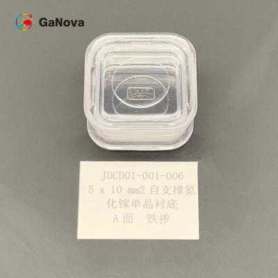
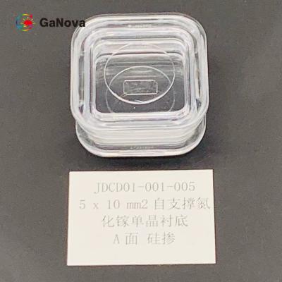
5*10mm2 A-Face Un-Doped SI-Type Free-Standing GaN Single Crystal Substrate Resistivity > 10⁶ Ω·Cm RF Devices Wafer
Price: Negotiable
MOQ: Negotiable
Delivery Time: 3-4 week days
Brand: GaNova
High Light:5*10mm2 GaN Single Crystal Substrate
5*10mm2 A-face Un-doped SI-type free-standing GaN single crystal substrate Resistivity > 106 Ω·cm RF devices wafer Overview Thin Epi wafers are commonly used for leading edge MOS devices. Thick Epi or Multi-layered epitaxial wafers are used for the devices mainly to control electric power, and th... View More
➤ Visit Website
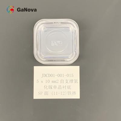
5*10mm2 SP-Face (11-12) Un-Doped SI-Type Free-Standing GaN Single Crystal Substrate Resistivity > 10⁶Ω·Cm RF Device
Price: Negotiable
MOQ: Negotiable
Delivery Time: 3-4 week days
Brand: GaNova
High Light:10⁶Ω·Cm GaN Single Crystal Substrate, 10mm2 GaN Single Crystal Substrate
5*10mm2 SP-face (11-12) Un-doped SI-type free-standing GaN single crystal substrate Resistivity > 106 Ω·cm RF devices wafer Overview The GaN semiconductor device market includes key companies such as Cree, Infineon Technologies, Qorvo, MACOM, NXP Semiconductors, Mitsubishi Electric, Efficient Pow... View More
➤ Visit Website
5*10mm2 A-face Un-doped n-type free-standing GaN single crystal substrate Resistivity < 0.05 Ω·cm Power device/laser
Price: Negotiable
MOQ: Negotiable
Delivery Time: 3-4 week days
Brand: GaNova
High Light:5*10mm2 GaN single crystal substrate
5*10mm2 A-face Un-doped n-type free-standing GaN single crystal substrate Resistivity < 0.05 Ω·cm Power device/laser wafer Overview Power density is greatly improved in gallium nitride devices compared to silicon ones because GaN has the capacity to sustain much higher switching frequencies. It a... View More
➤ Visit Website
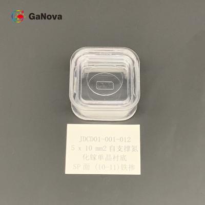
5*10mm2 SP-Face (10-11) Un-Doped SI-Type Free-Standing GaN Single Crystal Substrate Resistivity > 10⁶ Ω·Cm RF Device
Price: Negotiable
MOQ: Negotiable
Delivery Time: 3-4 week days
Brand: GaNova
High Light:10⁶ Ω·Cm GaN Single Crystal Substrate
5*10mm2 SP-face (10-11) Un-doped SI-type free-standing GaN single crystal substrate Resistivity > 106 Ω·cm RF devices wafer Now a new material called Gallium Nitride (GaN) has the potential to replace silicon as the heart of electronic chips. Gallium Nitride can sustain higher voltages than silic... View More
➤ Visit Website
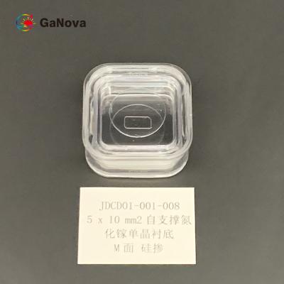
5*10mm2 M-Face Un-Doped N-Type Free-Standing GaN Single Crystal Substrate Resistivity < 0.05 Ω·cm Power Device/Laser
Price: Negotiable
MOQ: Negotiable
Delivery Time: 3-4 week days
Brand: GaNova
High Light:Laser GaN Single Crystal Substrate
5*10mm2 M-face Un-doped n-type free-standing GaN single crystal substrate Resistivity < 0.05 Ω·cm Power device/laser wafer Overview These GaN wafers realize unprecedented ultra-bright laser diodes and high-efficiency power devices for use in projector light sources, inverters for electric vehicle... View More
➤ Visit Website
AlGaN Buffer Thickness 600nm 2inch Blue-LED GaN On Silicon Wafer
Price: Negotiable
MOQ: Negotiable
Delivery Time: 3-4 week days
Brand: GaNova
High Light:600nm GaN On Silicon Wafer, 2inch GaN On Silicon Wafer
2inch Blue-LED GaN on silicon wafer There are three main substrates that are used with GaN - Silicon Carbide (SiC), Silicon (Si) and Diamond. GaN on SiC is the most common of the three and has been used in various applications in the Military and for High Power Wireless Infrastructure Applications. ... View More
➤ Visit Website
GaN Substrates Ga Face Surface Roughness < 0.2 nm (Polished) Or < 0.3 nm (Polished And Surface Treatment For Epitaxy)
Price: Negotiable
MOQ: Negotiable
Delivery Time: 3-4 week days
Brand: GaNova
High Light:Surface Treatment GaN Substrates, Epitaxy GaN Substrates, Polished GaN Substrates
10*10.5mm² C-face Un-doped n-type free-standing GaN single crystal substrate Resistivity < 0.1 Ω·cm Power device/laser Overview We provide high-quality GaN substrates which are produced by originally designed HVPE (Hydride Vapor Phase Epitaxy) method, utilizing more than 10 years of experience in... View More
➤ Visit Website

4 Inch N-Type Si-Doped GaN On Sapphire Wafer SSP Resistivity<0.05 Ω cm LED, Laser, PIN Epitaxial Wafer
Price: Negotiable
MOQ: Negotiable
Delivery Time: 3-4 week days
Brand: GaNova
High Light:Sapphire GaN Epitaxial Wafer, PIN GaN Epitaxial Wafer, 4 Inch GaN Epitaxial Wafer
4 inch N-type Si-doped GaN on sapphire wafer SSP resistivity<0.05 Ω cm LED, laser, PIN epitaxial wafer For lightly Si-doped GaN ([Si] = 2.1 × 1016 cm−3), the room temperature (RT) electron mobility was as high as 1008 cm2 V−1 s−1, which was dominantly limited by polar optical phonon scattering. More... View More
➤ Visit Website